Global Semiconductor Ecosystem: Insights into a $1 Trillion Industry
Semiconductors have become fundamental to modern life since the invention of the first transistor in 1947 by John Bardeen, Walter Brattain, and William Shockley at Bell Laboratories—and the subsequent development of the integrated circuit (IC) by Jack Kilby and Robert Noyce in 1958 and 1959, respectively. Yet, it wasn’t until the global chip shortage during the COVID-19 pandemic that the world fully recognized its pervasive and powerful presence. A closer look at our daily life reveals the extent of our reliance: a single smartphone contains approximately 169 chips, a coffee maker includes more than ten, and a standard automobile may incorporate anywhere from 1,000 to 3,500 semiconductor chips inside [1] .
Once viewed as the silent engine of the digital age, the semiconductor industry is now at the forefront of global transformation. The rise of artificial intelligence (AI) has significantly redefined market dynamics, innovation roadmaps, and capital allocation across the semiconductor value chain. At the same time, geopolitical tensions and national security concerns are disrupting global supply chains and triggering a reevaluation of industrial strategies.
This article offers a comprehensive overview of the semiconductor ecosystem—its structure, leading players, and broad range of applications—that are collectively reshaping the global semiconductor landscape.
Global Semiconductor ecosystem:
The global semiconductor ecosystem is a complex and interconnected network of companies and processes involved in the design, fabrication, assembly, testing, and distribution of semiconductor chips.
The global semiconductor ecosystem can be split into six segments-
- Design
- Wafer Fabrication
- Specialized Materials and Gases
- Equipment Manufacturer
- Packaging and Testing
- Sales & Distribution
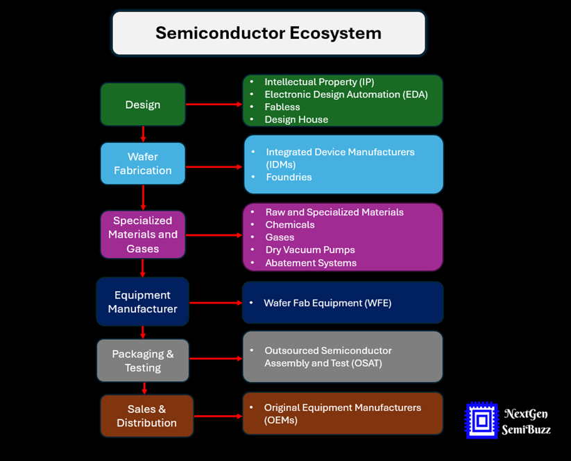
Fig-1: Global Semiconductor Ecosystem Overview
- Design
Semiconductor chip design is the encompassing process of defining, developing, and verifying all aspects of a semiconductor chip, from concept to final product. It involves multiple stages, including system specification, architecture design, logic design, physical design, verification, and validation. It translates market requirements and product specifications into a detailed and verified blueprint for the chip’s hardware implementation. The whole design process can be divided into four subcategories.
- Intellectual Property (IP)
- Electronic Design Automation (EDA)
- Fabless
- Design House
Intellectual Property (IP):
Semiconductor intellectual property (IP) comprises pre-designed, reusable blocks of logic, functionality, or layout licensed to multiple vendors. These IP blocks serve as essential building blocks in integrated circuit (IC) design, accelerating development by eliminating the need to design every function from scratch. Licensees typically pay either an upfront fee or royalties based on production volume. By providing validated, ready-to-use components, semiconductor IP streamlines chip design and enables teams to focus on system-level innovation and differentiation. Key categories include processor, interface, and memory IP, all of which are vital for applications across consumer, automotive, and industrial sectors.
The global Semiconductor IP market was valued at USD 47.91 billion in 2024 and is projected to reach USD 75.22 billion by 2031, growing at a CAGR of 6.4% during the forecast period from 2024 to 2031, reflecting the increasing demand for scalable and cost-efficient design solutions in the semiconductor ecosystem [2–3].
Current key players in Semiconductor Chip IP [4, 5, 6, 7]: Arm Holdings Ltd. (UK), Synopsys, Inc. (US), Cadence Design Systems, Inc. (US), Imagination Technologies (UK), CEVA, Inc. (US), Lattice Semiconductor (US), Rambus (US), eMemory Technology Inc. (Taiwan), VeriSilicon (China), Achronix Semiconductor Corporation (US), Silicon Storage Technology, Inc. (US), Alphawave SEMI (UK), ARTERIS, Inc (US).
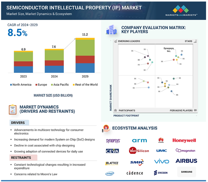
Fig-2: Semiconductor Intellectual Property (IP) market overview [7]
Electronic Design Automation (EDA):
Electronic Design Automation (EDA) [8–9] refers to a comprehensive suite of software tools and methodologies used by semiconductor engineers to design, simulate, verify, and prepare integrated circuits (ICs) for manufacturing. These tools are indispensable in managing the increasing complexity of modern chip design, automating critical processes such as schematic capture, layout design, functional verification, timing analysis, and physical implementation.
EDA solutions also enable the seamless integration of internal and third-party Intellectual Property (IP) blocks, supporting more efficient, scalable, and collaborative chip development workflows. As chip architectures grow more sophisticated, the dependence on EDA tools throughout the design lifecycle—from initial concept to final tape-out—has become increasingly vital.
According to the SNS Insider Report, the EDA market [10, 11, 12] was valued at USD 14.66 billion in 2023 and is expected to grow to USD 32.75 billion by 2032, registering a compound annual growth rate (CAGR) of 9.35% from 2024 to 2032. This growth is largely driven by breakthroughs in artificial intelligence (AI), machine learning (ML), and cloud-based design platforms, which are reshaping chip design by improving precision and scalability and reducing time to market.
Current key players in Semiconductor EDA [10]: Synopsys (Design Compiler, PrimeTime), Cadence Design Systems (Virtuoso, Allegro), Siemens EDA (Calibre, PADS), ANSYS (HFSS, RedHawk), Keysight Technologies (ADS, SystemVue), Zuken (CR-8000, E3.series), Altair Engineering (PollEx, HyperWorks), Autodesk (Fusion 360, Eagle), Altium (Altium Designer, CircuitStudio), Mentor Graphics (ModelSim, Questa), Silvaco (TCAD, SmartSpice), AWR Corporation (Microwave Office, Visual System Simulator), Magma Design Automation (Talc, Blast Fusion), Dassault Systèmes (3DEXPERIENCE, CATIA), National Instruments (Multisim, LabVIEW), ARM Holdings (Physical IP, CoreSight), Rambus (Design IP, Security IP), Xilinx (Vivado, ISE Design Suite), Intel (Quartus Prime, Pathfinder), Broadcom (IP Licensing, ASIC Design Services).
Fabless:
Fabless semiconductor companies [13] focus on the design, development, and marketing of integrated circuits (ICs), while outsourcing chip fabrication to specialized foundries. Unlike integrated device manufacturers (IDMs), fabless firms do not operate their own fabrication facilities, enabling them to direct resources toward innovation, R&D, and market expansion without the heavy capital investments required for manufacturing infrastructure.
Despite not owning fabs, these companies retain full ownership of their intellectual property and chip designs. They establish the technical specifications and quality standards that foundries must adhere to, ensuring high-performance and reliable products.
This asset-light model allows fabless companies [14] to remain agile, rapidly adapt to shifting market demands, and leverage cutting-edge manufacturing technologies from global foundry partners. As a result, they play a vital role in driving innovation and technological advancement across the semiconductor industry.
The global fabless semiconductor market [15] is projected to grow from USD 214.5 billion in 2024 to approximately USD 489 billion by 2034, reflecting a compound annual growth rate (CAGR) of 8.60%. In 2024, the Asia-Pacific region led the market with a 58.61% share, generating USD 125 billion in revenue. Within this region, China’s fabless market was valued at USD 43.62 billion and is expected to grow at a CAGR of 8.72% over the same period.
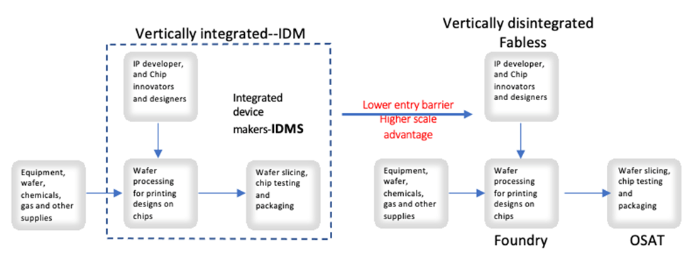
Fig-3: Fabless business model [16]
Top Fabless companies include Nvidia Corporation, Intel FPGA, Qualcomm Inc., Broadcom Inc., AMD, MediaTek Inc., Marvell Technology, Inc., Realtek Semiconductor Corporation, Novatek Microelectronics Corp., Cirrus Logic [17].
Design House:
A design house is a specialized service provider that offers chip design solutions, often serving as a crucial intermediary between fabless semiconductor companies and foundries. These firms play a key role in adapting and optimizing integrated circuit (IC) designs to meet the specific process requirements of manufacturing partners, with a strong emphasis on back-end design tasks such as physical layout, verification, and design for manufacturability (DFM).
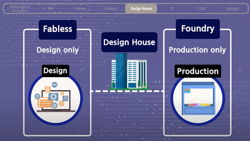
Fig-4: Relationship overview of Design House with Fabless and Foundry [18]
Design houses focus on ensuring that chip designs developed by fabless companies are compatible with the target foundry’s capabilities, thereby facilitating a smooth and efficient handoff for mass production. While they contribute significantly to the manufacturability and performance of semiconductor devices, design houses typically do not own the intellectual property (IP) of the chips they work on. Instead, they operate on a project basis, offering deep technical expertise to support successful design transfers from concept to silicon. By leveraging their in-depth understanding of specific foundry technologies and process nodes, design houses enhance the effectiveness of the fabless business model, helping product developers reduce design cycles, lower costs, and improve production yields.
Although design houses often operate behind the scenes and may not have the same public visibility as fabless companies or foundries, they are integral to the semiconductor supply chain. Prominent players in this space include GlobalFoundries, Synopsys, Cadence Design Systems, Arm, Alchip Technologies, eMemory Technology, and Global Unichip Corporation, among others.
Fabless companies are product developers, while design houses are service providers, enabling those product developers to translate their designs into physical chips using external manufacturing facilities.
2. Wafer Fabrication
Wafer fabrication is one of the most critical and complex processes in the semiconductor industry, transforming integrated circuit (IC) designs into functional silicon chips. It is the stage where chip designs are physically realized, involving hundreds of highly precise and controlled steps to build complex circuits on a silicon wafer. Key processes in wafer fabrication [19–20] include oxidation, photolithography and patterning, etching, doping and ion implantation, deposition, metallization and interconnect formation, as well as passivation and encapsulation. Each of these steps requires advanced technologies and meticulous control to ensure accuracy and consistency.
Due to the intricate nature of the process and the high level of precision required, fabricating a single wafer can take several weeks to months. For advanced nodes, such as 3nm chips, the fabrication cycle can span 3 to 4 months. In contrast, older process nodes with fewer layers and steps typically have shorter cycle times [21–22]. The extended duration and complexity of wafer fabrication are driven by the need for extreme precision, stringent quality control, and the pursuit of high yields in the final product. Even minor deviations at any stage can impact performance, reliability, or yield, making process optimization crucial.
Wafer fabrication is carried out either by Integrated Device Manufacturers (IDMs)—which handle design and manufacturing in-house—or by specialized foundries, which manufacture chips on behalf of fabless companies.
Integrated Device Manufacturers (IDMs):
Integrated Device Manufacturers (IDMs) are semiconductor companies that design, manufacture, and sell their own integrated circuit (IC) products. Unlike fabless companies, which outsource production to foundries, IDMs own and operate their fabrication facilities (fabs) and manage the entire semiconductor manufacturing process, from design to mass production.
This vertically integrated model provides IDMs with greater control over production timelines, quality assurance, and supply chain logistics. With both design and manufacturing in-house, IDMs can achieve faster iteration cycles, enhanced coordination between R&D and production, and potential cost efficiencies. This tight integration often results in a more synchronized approach to innovation, enabling IDMs to respond quickly to market demands and technological advancements.
Leading Integrated Device Manufacturers (IDMs) [23–24] are – Samsung Electronics, Intel Corporation, SK Hynix, Micron Technology, Texas Instruments, Infineon Technologies, STMicroelectronics, and NXP Semiconductors.
Foundries:
Semiconductor foundries are specialized manufacturing facilities dedicated to producing integrated circuits (ICs)—commonly known as chips—on behalf of other companies. Often referred to as the “factories” of the semiconductor industry, foundries play a pivotal role in the global semiconductor supply chain. They enable fabless companies, which focus solely on chip design, to manufacture their designs without the massive capital investment required to build and operate fabrication facilities. Unlike Integrated Device Manufacturers (IDMs), foundries do not design chips; they manufacture semiconductors exclusively based on the design specifications provided by their clients.
Foundries specialize in high-volume, high-precision chip fabrication, often utilizing cutting-edge process nodes such as 5nm, 3nm, or even sub-3nm technologies. Their focus is on delivering manufacturing excellence, yield optimization, and technology scalability to a diverse client base across consumer electronics, automotive, data center, and AI sectors.
The foundry business model is a pure-play manufacturing model, characterized by B2B Service Provider, Technology Licensing & Process Specialization, Economies of Scale, Tiered Client Relationships and Strategic Partnerships.
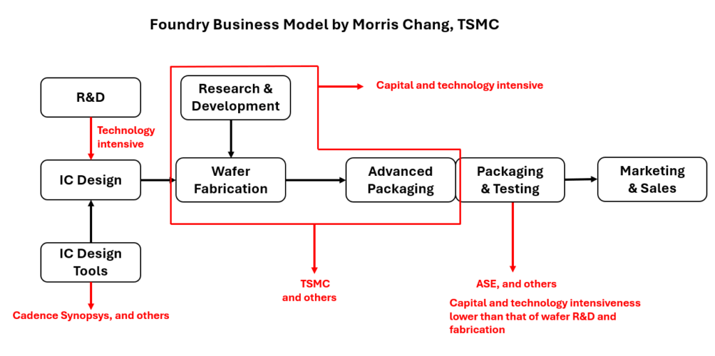
Fig-5: Foundry business model by Morris Chang [25]
Leading Semiconductor Foundries are [26–27] – Taiwan Semiconductor Manufacturing Company -TSMC (Taiwan), Samsung Foundry (South Korea), GlobalFoundries (USA), United Microelectronics Corporation- UMC (Taiwan), Semiconductor Manufacturing International Corporation – SMIC (China).
Other Notable Foundries: Hua Hong Semiconductor (China), Tower Semiconductor (USA), and Vanguard International Semiconductor Corporation – VIS (Taiwan).
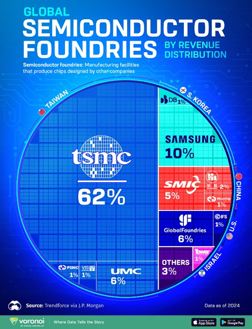
Fig-6: Global Semiconductor Foundries Revenue Model [28].
3. Specialized Materials and Gases:
Semiconductor chip fabrication relies on a wide array of raw materials, specialty chemicals, process gases, dry vacuum pumps, and abatement systems. These components are essential for executing the precise and complex steps involved in wafer processing. A specialized network of suppliers supports the industry by providing these critical materials and equipment, ensuring consistency, purity, and reliability throughout the manufacturing process.
Raw and Specialized Materials:
Semiconductor fabrication is highly dependent on both raw and specialized materials that enable the intricate processes involved in chip manufacturing [29]. Raw materials such as silicon, germanium, gallium arsenide, and indium phosphide serve as the foundational substrates for integrated circuits. In addition, specialized materials—such as dopants (e.g., boron, phosphorus, arsenic), conductive metals for interconnects, and insulating compounds like silicon dioxide and silicon nitride—are essential for defining electrical properties and ensuring device performance [30]. According to market data, the global semiconductor materials market was valued at USD 69.39 billion in 2024 and is projected to grow to USD 96.24 billion by 2032, registering a compound annual growth rate (CAGR) of 4.2% during the forecast period [31].
A critical subset of this market is the silicon wafer industry, which forms the backbone of chip fabrication. Valued at approximately USD 12 billion in 2023, this sector continues to evolve rapidly as demand for smaller, faster, and more power-efficient chips increases [32]. Advancements in wafer manufacturing technologies are essential to meet the stringent requirements of next-generation semiconductor devices. Moreover, the global semiconductor wafer market was valued at USD 20.23 billion in 2023 and is expected to rise to USD 32.57 billion by 2032, growing at a CAGR of 5.43% between 2025 and 2032 [33]. This growth underscores the escalating demand for high-purity, high-precision wafers across various applications.
Leading players in the silicon wafer manufacturing segment include WaferPro, SUMCO, Shin-Etsu, SK Siltron, and Siltronic AG [33].
Chemicals:
The semiconductor fabrication industry is heavily reliant on the specialty chemical sector, which supplies the critical high-purity materials required for manufacturing integrated circuits (ICs)[34]. These chemicals play a fundamental role in various fabrication stages, including etching, cleaning, deposition, and doping, all which demand precision, consistency, and contamination-free environments.
Specialty chemical companies are instrumental in meeting these requirements by developing advanced chemical formulations tailored specifically for semiconductor manufacturing processes. Notable players in this field include BASF SE, Dow Inc., JSR Corporation, Fujifilm Holdings Corporation, Merck KGaA, and Honeywell International Inc., each known for their expertise in producing semiconductor-grade materials.
According to industry data, the global semiconductor chemicals market was valued at USD 12.2 billion in 2023 and is projected to reach USD 21.9 billion by 2028, growing at a compound annual growth rate (CAGR) of 12.3% during the forecast period [35]. This strong growth is being driven by the rising demand for advanced electronic devices, which has significantly increased global semiconductor production. As fabrication technologies evolve to accommodate smaller nodes and more complex chip architectures, the demand for high-quality, ultra-pure chemicals continues to escalate.
Gases:
The semiconductor fabrication industry depends heavily on ultra-high-purity gases—both bulk and specialty—for critical manufacturing processes such as etching, deposition, and cleaning. These gases are essential for ensuring process precision and product quality in advanced chip production.
Leading global gas suppliers include Air Liquide, Air Products and Chemicals, Linde plc, Matheson Tri-Gas, Taiyo Nippon Sanso, SK Materials, American Gas Products, Electronic Fluorocarbons, Iwatani Corporation, Showa Denko K.K., and Messer Group. The sector demands significant technical expertise and capital investment to meet the stringent purity requirements of semiconductor manufacturing. The global semiconductor gases market was valued at USD 10.07 billion in 2023 and is expected to grow to USD 19.34 billion by 2032, at a CAGR of 7.5% [36]. Asia Pacific led the market with a 73.68% share in 2023, while the U.S. market is projected to reach USD 1.73 billion by 2032, driven by rising demand for advanced electronics and increased investment in domestic semiconductor capabilities.
Dry Vacuum Pumps:
Vacuum-based process systems are integral to semiconductor manufacturing, supporting critical upstream and downstream operations such as chemical vapor deposition (CVD), etching, and ion implantation. These systems rely on high-performance dry vacuum pumps to maintain the controlled environments essential for precision fabrication.
The global vacuum pump market was valued at USD 6.31 billion in 2024 and is projected to reach USD 10.08 billion by 2031, growing at a CAGR of 6.66% during the forecast period [37]. Key players in the dry vacuum pump industry [38] include Agilent Technologies, Alfa Laval, Atlas Copco, Becker Vacuum Pumps, DEKKER Vacuum Technologies, Ebara Corporation, Edwards Vacuum, Flowserve Corporation, Graham Corporation, Grundfos, KNF Neuberger, Leybold GmbH, Tuthill Corporation, ULVAC, and Welch Vacuum.
Abatement Systems:
Abatement systems, also known as exhaust abatement systems, are critical components in semiconductor fabrication (semi-fab) facilities. These systems neutralize and safely manage toxic, flammable, and environmentally hazardous gases generated during chip production, ensuring emissions comply with national regulations and protecting both human health and the environment [39–40]. The global semiconductor abatement systems market was valued at USD 1.13 billion in 2024 and is projected to reach USD 2.83 billion by 2033, growing at a CAGR of 10.8% during the forecast period [41].
Key players in this market [42] include Edwards Vacuum (Atlas Copco), Ebara Corporation, CS Clean Systems, DAS Environmental Expert, Ecosys Abatement, Nippon Sanso, Showa Denko, and Exentec.
4. Equipment Manufacturer
Wafer Fab Equipment (WFE) refers to the specialized machinery and tools used in semiconductor fabrication facilities to manufacture integrated circuits, microchips, and other semiconductor devices. WFE supports a wide range of highly complex and precise processes, including [43]:
- Wafer Manufacturing/Wafer Processing,
- Fab Facilities Equipment,
- Mask/Reticle Equipment,
- Surface Conditioning/ Clean and Dry,
- Resist Processing Equipment,
- Expose and Write,
- Etch Equipment (Dry etch, Wet etch),
- Sputter Equipment,
- Thermal Processing Equipment,
- Chemical Mechanical Planarization (CMP),
- Chemical Vapor Deposition (CVD),
- Inspection Measurement,
- Assembly and Packaging Equipment,
- SOC & Logic Test Equipment,
- Memory Test Equipment,
- Handlers,
- Probe Equipment, and
- Other Test Related Equipment.
Advancements in WFE—such as High NA EUV lithography [44]—have enabled the development of smaller, faster, and more power-efficient chips. These tools are fundamental to high-volume semiconductor manufacturing, ensuring production efficiency, high yields, and device reliability.
The WFE industry is led by key players [45] including ASML Holding NV, Applied Materials Inc., Tokyo Electron Limited (TEL), Lam Research Corporation, KLA Corporation, Screen Holdings Co., Ltd., Hitachi High-Tech Corporation, Advantest Corporation, Teradyne Inc., and ASM International NV.
The global semiconductor manufacturing equipment market is expected to maintain strong growth, reaching $121 billion in 2025, $139 billion in 2026 [46], and surpassing $165 billion by 2029 [47], driven by robust demand across both front-end and back-end segments.

Fig-7: Global Wafer Fab Equipment (WFE) industry report [48].
5. Packaging and Testing
Outsourced Semiconductor Assembly and Test (OSAT) providers specialize in delivering semiconductor packaging, assembly, and testing services to other companies in the semiconductor industry [49]. OSATs play a pivotal role in the semiconductor value chain by bridging the gap between semiconductor manufacturing (foundries) and the final integration of chips into electronic devices. These companies play a critical role in the semiconductor supply chain by enabling cost-effective, high-quality post-fabrication processes. This allows semiconductor firms to concentrate on their core competencies such as chip design and wafer fabrication, while OSAT providers manage the complex downstream processes.
The OSAT market is geographically concentrated in the Asia-Pacific region, with key operations in Taiwan, China, and South Korea [50]. To meet the increasing demand for compact, high-performance devices, OSATs are rapidly adopting advanced packaging technologies such as fan-out wafer-level packaging (FOWLP) and 3D packaging.
As semiconductor devices grow in complexity—integrating multiple functionalities into smaller form factors—the need for specialized assembly and testing capabilities is driving sustained OSAT market growth.
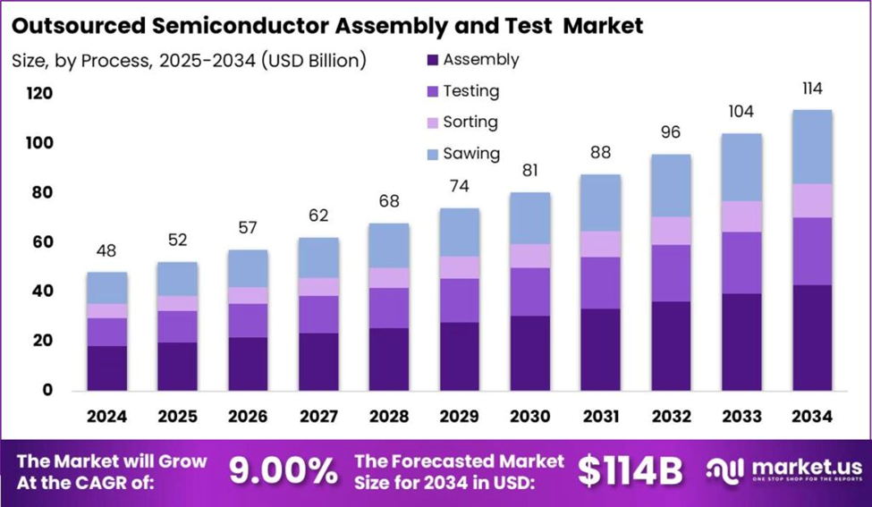
Fig-8: Outsourced Semiconductor Assembly and Test (OSAT) Market [51]
According to Valuates Reports, the global OSAT market was valued at USD 66.1 billion in 2024 and is projected to reach USD 93.8 billion by 2031, growing at a CAGR of 5.2% during the forecast period. [52].
Leading OSAT providers include [49]: ASE Technology Holding Group, Amkor Technology Inc., Powertech Technology Inc., Chipmos Technologies Inc., King Yuan Electronics Co. Ltd, Formosa Advanced Technologies Co. Ltd, Jiangsu Changjiang Electronics Technology Co. Ltd, UTAC Holdings Ltd, Lingsen Precision Industries Ltd, Tongfu Microelectronics Co., Chipbond Technology Corporation, Hana Micron Inc., Integrated Micro-electronics Inc., and Tianshui Huatian Technology Co. Ltd.
6. Sales & Distribution:
Original Equipment Manufacturers (OEMs) play a pivotal role in the semiconductor industry’s sales and distribution network [53]. OEMs [54] purchase semiconductor components—such as microprocessors, memory, or sensors—and integrate them into end-user products like smartphones, computers, vehicles, and industrial systems. While the final products carry the OEMs’ brand names, the embedded semiconductor technologies often originate from external suppliers.
OEMs not only act as major consumers of semiconductor components but also influence technological development and product roadmaps through their evolving performance and integration requirements. Their strategic decisions and demand patterns significantly shape the production planning and innovation cycles of semiconductor manufacturers.
Serving as a bridge between chipmakers and end markets, OEMs are central to the semiconductor value chain. Their scale, specialization, and product diversity drive a complex global distribution ecosystem that ensures semiconductor technologies reach diverse application sectors efficiently.
According to SEMI’s OEM Perspective at SEMICON West 2024, global sales of semiconductor manufacturing equipment by OEMs are expected to reach a record $109 billion in 2024, marking a 3.4% year-over-year increase [55]. This momentum is projected to continue, with equipment sales forecast to hit $128 billion in 2025, fueled by robust demand across both front-end and back-end segments of the manufacturing process.
Some examples of Original Equipment Manufacturers (OEMs) that are significant players in the semiconductor ecosystem:
- Consumer Electronics:
- Smartphones & Mobile Devices: Apple, Samsung Electronics, Xiaomi, Huawei, Oppo, Vivo.
- Computing (PCs, Laptops, Tablets): Lenovo, Dell, HP Inc., Apple.
- Gaming Consoles & Entertainment Devices: Sony (PlayStation), Microsoft (Xbox), Nintendo.
- Wearable Devices (Smartwatches, Fitness Trackers): Apple, Samsung Electronics, Garmin, Fitbit.
- Other Consumer Electronics: LG Electronics, Samsung Electronics, Sony.
- Automotive:
- Electric Vehicle Manufacturers (EVs): Tesla, BYD, Rivian, Lucid.
- Traditional Automakers (ICE Vehicles & Hybrid): Volkswagen Group, Toyota, General Motors, Ford.
- Industrial & Other Specialized Sectors:
- Industrial Automation & Equipment: Siemens, ABB, Mitsubishi Electric.
- Aerospace & Defense: Lockheed Martin, Boeing, Raytheon Technologies.
- Medical Devices: Medtronic, Johnson & Johnson, Philips Healthcare.
- Data Centers: Amazon Web Services (AWS), Microsoft Azure, Google Cloud, Meta.
Fig-9: One Giant Chart – The Value of the Global Semiconductor Industry [56].
In conclusion, the global semiconductor ecosystem is rapidly evolving, driven by innovation, collaboration, and growing demand across industries. With the market size surpassing USD 584.17 billion in 2024 and projected to reach approximately $1,137.57 billion (~ $1.14 trillion) by 2033 at a CAGR of 7.64% [57], the industry is poised for significant growth. It is driven by innovation and shaped by trends such as AI, electrification, and digital transformation, with Asia, the U.S., and Europe playing pivotal regional roles. Collaboration, supply chain resilience, and technological leadership are key to sustaining its growth and competitiveness [58].
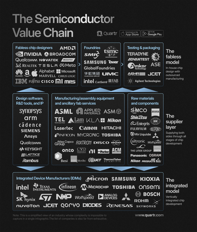
Fig-10: An infographic depicting the semiconductor value chain [58].
About the Author!
Dr. Akter is a dynamic and results-driven engineering professional with a multifaceted background in the semiconductor industry, telecom project management, and strategic volunteer leadership. She has proven expertise in enhancing process stability, optimizing yield, and improving manufacturing capabilities as a former Module Development Engineer at Intel and Yield Analysis Engineer at Micron. Her strong academic foundation, reinforced by a Ph.D. in Electrical and Computer Engineering, complements a track record of leading complex projects, driving innovation, and delivering high-impact results. Dr. Akter’s extensive experience has honed her skills in nano/micro-fabrication, characterization, advanced data analysis, and emerging technologies such as Generative AI and Machine Learning. Certified in PMP and a Lean Six Sigma Black Belt, she excels in data-driven decision-making, operational efficiency, and cross-functional team leadership. Dr. Akter is adept at leveraging advanced analytical tools to troubleshoot challenges, implementing strategic initiatives, and drive continuous improvement.